- 您现在的位置:买卖IC网 > Sheet目录308 > ADUM6132ARWZ-RL (Analog Devices Inc)IC GATE DRIVER ISOLATED 16-SOIC
�� �
�
�ADuM6132�
�In� applications� involving� high� common-mode� transients,� care�
�should� be� taken� to� ensure� that� board� capacitive� coupling� across�
�the� isolation� barrier� is� minimized.� Furthermore,� the� board�
�layout� should� be� designed� so� that� any� coupling� that� does� occur�
�affects� all� pins� on� a� given� component� side� equally.� Failure� to�
�ensure� this� may� cause� voltage� differentials� between� pins� that�
�exceed� the� absolute� maximum� ratings� of� the� device� (see� Table� 7),�
�leading� to� latch-up� or� permanent� damage.�
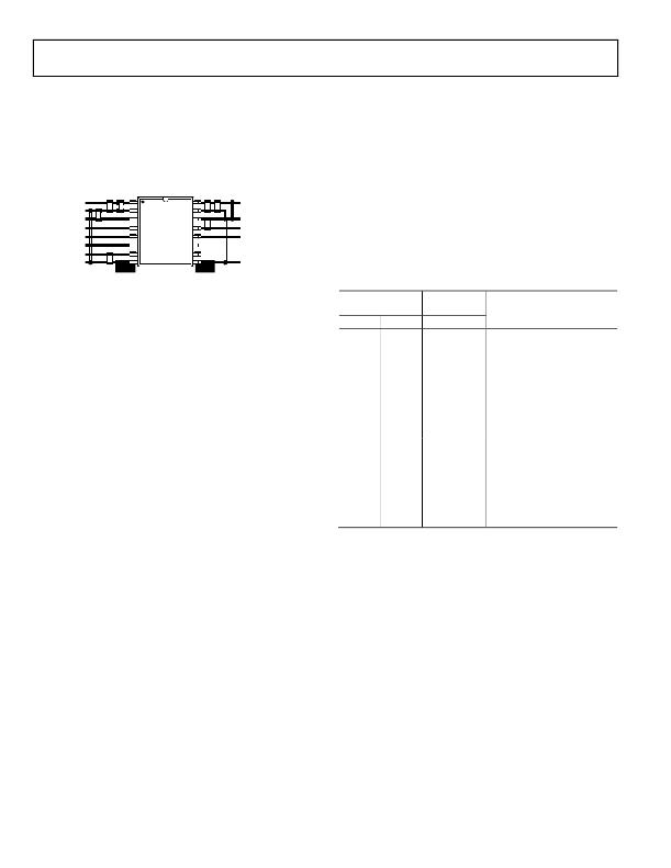
�V� DD� V� ISO�
�GND� GND� ISO�
�Data� Sheet�
�UNDERVOLTAGE� LOCKOUT�
�The� ADuM6132� has� undervoltage� lockout� (UVLO)� circuits� on�
�the� V� DDL� ,� V� DDA� ,� and� V� DDB� supplies.� For� each� supply,� the� respective�
�UVLO� circuit� monitors� the� supply� voltage� and� takes� a� predeter-�
�mined� action� based� on� whether� the� supply� voltage� is� above� or�
�below� a� given� threshold.� These� thresholds� are� specified� in� Table� 1.�
�In� the� recommended� configuration� shown� in� Figure� 16,� only�
�two� independent� supplies� are� controlled� by� the� user:� V� DDB� and�
�V� DDL� /V� DD� (V� DDL� =� V� DD� in� Figure� 16).� V� DDA� is� supplied� by� the�
�V� DDL�
�V� IA�
�V� IB�
�V� OB�
�V� DDB�
�GND�
�Figure� 17.� Recommended� PCB� Layout�
�GND� A�
�V� DDA�
�V� OA�
�NC�
�NC�
�GND� ISO�
�internal� dc-to-dc� converter� via� the� V� ISO� =� V� DDA� external� connec-�
�tion.� Nevertheless,� the� V� DDA� UVLO� functionality� is� included� in�
�Table� 11� to� show� how� the� V� OA� output� behaves� when� the� internal�
�dc-to-dc� converter� powers� on� and� off.�
�Table� 11.� Undervoltage� Lockout� Functionality� 1�
�The� ADuM6132� is� a� power� device� that� dissipates� approximately�
�1� W� of� power� when� fully� loaded� and� running� at� maximum� speed.�
�Because� it� is� not� possible� to� apply� a� heat� sink� to� an� isolation�
�device,� the� device� depends� primarily� on� heat� dissipation� into�
�the� PCB� through� the� GND� pins.� If� the� device� will� be� used� at�
�high� ambient� temperatures,� provide� a� thermal� path� from� the�
�GND� pins� to� the� PCB� ground� plane.�
�The� board� layout� in� Figure� 17� shows� enlarged� pads� for� Pin� 8�
�(GND)� and� Pin� 9� (GND� ISO� ).� Multiple� vias� should� be� implemented�
�from� the� pad� to� the� ground� plane.� This� layout� significantly� reduces�
�the� temperatures� inside� the� chip.� The� dimensions� of� the� expanded�
�pads� are� left� to� the� discretion� of� the� designer� and� the� available�
�board� space.� See� the� AN-0971� Application� Note� for� board�
�layout� recommendations.�
�User-Provided�
�Supplies�
�V� DDL� V� DDB�
�H� H�
�H� H�
�X� L�
�V� ISO� Powered�
�Supply�
�V� DDA�
�H�
�L�
�X�
�Effect�
�Normal� operation.�
�Internal� dc-to-dc� converter� is�
�active.�
�V� OA� /V� OB� output� logic� states�
�match� V� IA� /V� IB� input� logic� states.�
�Internal� dc-to-dc� converter� is�
�active� but� V� ISO� is� below� UVLO�
�threshold.�
�V� OA� output� is� driven� low.�
�V� OB� output� operates� normally.�
�Internal� dc-to-dc� converter� is�
�turned� off� (V� ISO� =� 0� V).�
�V� OA� output� is� driven� low.�
�V� OB� output� is� driven� low.�
�THERMAL� ANALYSIS�
�L�
�X�
�X�
�Internal� dc-to-dc� converter� is�
�turned� off� (V� ISO� =� 0� V).�
�The� ADuM6132� consists� of� several� internal� die� attached� to�
�two� lead� frame� paddles.� For� the� purposes� of� thermal� analysis,�
�V� OA� output� is� driven� low.�
�V� OB� output� is� driven� low.�
�the� part� is� treated� as� a� thermal� unit� with� the� highest� junction�
�temperature� determining� θ� JA� ,� as� shown� in� Table� 2.� The� value� of�
�1�
�H:� supply� voltage� >� UVLO� threshold;� L:� supply� voltage� <� UVLO� threshold;�
�X:� supply� voltage� level� is� irrelevant.�
�θ� JA� is� based� on� measurements� taken� with� the� part� mounted� on�
�a� JEDEC� standard� 4-layer� board� with� fine� width� traces� and� still�
�air.� Under� normal� operating� conditions,� the� ADuM6132� oper-�
�ates� at� full� load� across� the� full� temperature� range� without� derating�
�the� output� current.� However,� following� the� recommendations� in�
�the� PCB� Layout� section� decreases� the� thermal� resistance� to� the�
�PCB,� allowing� increased� thermal� margin� at� high� ambient�
�temperatures.�
�Under� V� ISO� output� short-circuit� conditions,� as� shown� in�
�Figure� 9,� the� package� power� dissipation� quickly� exceeds� the� safe�
�operating� limit� of� 1.44� W� for� ambient� temperatures� up� to� 85°C.�
�At� low� input� voltage,� the� power� dissipation� can� approach� 2� W.�
�Because� internal� compensation� of� the� PWM� makes� low� V� DD� a�
�worst-case� condition,� input� voltage� limiting� is� not� an� effective�
�strategy� for� protecting� the� ADuM6132� from� output� load� fault�
�conditions.� Therefore,� the� preferred� protection� methods,� where�
�When� all� three� supplies� are� above� their� respective� UVLO�
�thresholds,� the� ADuM6132� operates� normally.� The� internal�
�dc-to-dc� converter� is� active,� and� both� outputs� operate� as�
�determined� by� their� respective� input� logic� signals.� If� either� of�
�the� user-provided� supplies� is� below� its� UVLO� threshold,� the�
�ADuM6132� is� put� into� a� disabled� mode.� In� this� mode,� the�
�internal� dc-to-dc� converter� is� turned� off� and� both� outputs� are�
�driven� low.�
�The� V� OB� output� is� driven� low� by� either� the� V� DDL� or� V� DDB�
�UVLO� circuit� (whichever� is� below� its� threshold).� The� V� OA�
�output� is� driven� low� when� the� internal� dc-to-dc� converter� is�
�turned� off.� The� V� ISO� supply� voltage� drops� to� 0� V,� causing� V� DDA�
�to� drop� also� because� V� ISO� and� V� DDA� are� externally� connected.�
�When� V� DDA� is� below� its� UVLO� threshold,� the� V� DDA� UVLO�
�circuit� drives� V� OA� low.�
�required,� are� either� limiting� ambient� temperature� to� 60°C� or� the�
�use� of� a� fuse.�
�Rev.� B� |� Page� 12� of� 16�
�发布紧急采购,3分钟左右您将得到回复。
相关PDF资料
ADUM6201CRIZ
ISOLATED DC-DC CONV 2CH 16SOIC
ADUM6404ARWZ
IC ISOLATOR 4CH DCDC CONV 16SOIC
ADUM7241CRZ-RL7
ISOLATOR DGTL 1KVRMS 2CH 8SOIC
ADUM7440CRQZ-RL7
IC DIGITAL ISOLATOR 4CH 16QSOP
ADUM7510BRQZ
IC DGTL ISOLATOR 5CH 16QSOP
ADZS-21364-EZLITE
KIT EVAL EZ LITE ADDS-21364
ADZS-21371-EZLITE
KIT EVAL EZLITE ADZS-21371
ADZS-21469-EZLITE
KIT EVAL EZ LITE ADSP-21469
相关代理商/技术参数
ADUM6200
制造商:AD 制造商全称:Analog Devices 功能描述:Dual-Channel, 5 kV Isolators with Integrated DC-to-DC Converter
ADUM6200ARIZ
功能描述:IC ISOLATOR DGTL 2CH 16SOIC RoHS:是 类别:隔离器 >> 数字隔离器 系列:IsoPower®, iCoupler® 产品培训模块:IsoLoop® Isolator 标准包装:50 系列:IsoLoop® 输入 - 1 侧/2 侧:5/0 通道数:5 电源电压:3 V ~ 5.5 V 电压 - 隔离:2500Vrms 数据速率:110Mbps 传输延迟:12ns 输出类型:CMOS 封装/外壳:16-SOIC(0.154",3.90mm 宽) 供应商设备封装:16-SOIC N 包装:管件 工作温度:-40°C ~ 85°C 其它名称:390-1053-5
ADUM6200ARIZ-RL
功能描述:IC ISOLATOR DGTL 2CH 16SOIC RoHS:是 类别:隔离器 >> 数字隔离器 系列:IsoPower®, iCoupler® 产品培训模块:IsoLoop® Isolator 标准包装:50 系列:IsoLoop® 输入 - 1 侧/2 侧:5/0 通道数:5 电源电压:3 V ~ 5.5 V 电压 - 隔离:2500Vrms 数据速率:110Mbps 传输延迟:12ns 输出类型:CMOS 封装/外壳:16-SOIC(0.154",3.90mm 宽) 供应商设备封装:16-SOIC N 包装:管件 工作温度:-40°C ~ 85°C 其它名称:390-1053-5
ADUM6200ARWZ
功能描述:ISOLAT DGTL 5KVRMS 2CH 16SOIC-W RoHS:是 类别:隔离器 >> 数字隔离器 系列:IsoPower®, iCoupler® 产品培训模块:IsoLoop® Isolator 标准包装:50 系列:IsoLoop® 输入 - 1 侧/2 侧:5/0 通道数:5 电源电压:3 V ~ 5.5 V 电压 - 隔离:2500Vrms 数据速率:110Mbps 传输延迟:12ns 输出类型:CMOS 封装/外壳:16-SOIC(0.154",3.90mm 宽) 供应商设备封装:16-SOIC N 包装:管件 工作温度:-40°C ~ 85°C 其它名称:390-1053-5
ADUM6200ARWZ-RL
功能描述:隔离器接口集成电路 kV 2-Ch Isolator w/ Int DC/DC Converter RoHS:否 制造商:Texas Instruments 通道数量:2 传播延迟时间: 电源电压-最大:5.5 V 电源电压-最小:3 V 电源电流:3.6 mA 功率耗散: 最大工作温度:+ 125 C 安装风格: 封装 / 箱体:SOIC-8 封装:Tube
ADUM6200CRIZ
功能描述:ISOLATED DC-DC CONV 2CH 16SOIC RoHS:是 类别:隔离器 >> 数字隔离器 系列:IsoPower®, iCoupler® 产品培训模块:IsoLoop® Isolator 标准包装:50 系列:IsoLoop® 输入 - 1 侧/2 侧:5/0 通道数:5 电源电压:3 V ~ 5.5 V 电压 - 隔离:2500Vrms 数据速率:110Mbps 传输延迟:12ns 输出类型:CMOS 封装/外壳:16-SOIC(0.154",3.90mm 宽) 供应商设备封装:16-SOIC N 包装:管件 工作温度:-40°C ~ 85°C 其它名称:390-1053-5
ADUM6200CRIZ-RL
功能描述:IC ISOLATOR DGTL 2CH 16SOIC RoHS:是 类别:隔离器 >> 数字隔离器 系列:IsoPower®, iCoupler® 产品培训模块:IsoLoop® Isolator 标准包装:50 系列:IsoLoop® 输入 - 1 侧/2 侧:5/0 通道数:5 电源电压:3 V ~ 5.5 V 电压 - 隔离:2500Vrms 数据速率:110Mbps 传输延迟:12ns 输出类型:CMOS 封装/外壳:16-SOIC(0.154",3.90mm 宽) 供应商设备封装:16-SOIC N 包装:管件 工作温度:-40°C ~ 85°C 其它名称:390-1053-5
ADUM6200CRWZ
功能描述:ISOLAT DGTL 5KVRMS 2CH 16SOIC-W RoHS:是 类别:隔离器 >> 数字隔离器 系列:IsoPower®, iCoupler® 产品培训模块:IsoLoop® Isolator 标准包装:50 系列:IsoLoop® 输入 - 1 侧/2 侧:5/0 通道数:5 电源电压:3 V ~ 5.5 V 电压 - 隔离:2500Vrms 数据速率:110Mbps 传输延迟:12ns 输出类型:CMOS 封装/外壳:16-SOIC(0.154",3.90mm 宽) 供应商设备封装:16-SOIC N 包装:管件 工作温度:-40°C ~ 85°C 其它名称:390-1053-5